 | –≠–ª–µ–∫—Ç—Ä–æ–Ω–Ω—ã–π –∫–æ–º–ø–æ–Ω–µ–Ω—Ç: AKD4356 | –°–∫–∞—á–∞—Ç—å:  PDF PDF  ZIP ZIP |

ASAHI KASEI
[AKD4356]
<KM060602>
'99/11
- 1 -
GENERAL DESCRIPTION
The AKD4356 is an evaluation board for AK4356, the 24bit 6ch D/A converter for DVD-audio. The
AKD4356 has the interface with AKM's wave generator using ROM data and with AKM's A/D converter
evaluation boards. Therefore, it is easy to evaluate the AK4356. The AKD4356 also has the digital audio
interface and can achieve the interface with digital audio systems via opt-connector or RCA connector.
n
Ordering guide
AKD4356
---
Evaluation board for AK4356
(Cable for connecting with printer port of IBM-AT compatible PC
and control software are packed with this.)
FUNCTION
∑
On-board 2nd order LPF
∑
On-board clock generator
∑
Compatible with 3 types of interface
- Direct interface with AKM's A/D converter evaluation boards
and direct interface with AKM's signal generator(AKD43XX) by 10pin header
- On-board CS8414 as DIR which accepts optical input
- Direct interface with AC3 decoder by 10pin header
∑
BNC connector for an external clock input
∑
10pin header for serial control interface
DVDD = 4.5
5.25V
GND
CS8414
(DIR)
Opt In
A/D, D/A Data
ROM Data
Clock
Generator
AK4356
Rch
x3
AVDD = 4.5
5.25V
10pin Header
RCA In
Lch
x3
Output
LPF
10pin Header
Control Data
Figure 1. AKD4356 Block Diagram
* Circuit diagram and PCB layout are attached at the end of this manual.
Evaluation board Rev.B for AK4356
AKD4356

ASAHI KASEI
[AKD4356]
<KM060602>
'99/11
- 2 -
n
External analog circuit
The 2nd order LPF (fc=93.2kHz, Q=0.712) which adds differential outputs of AK4356 is implemented on the board.
When the further attenuation of the out-band noise is needed, some additional LPF is required. Analog signal is output
through BNC connectors on the board. And the output level of AK4356 is 5.5Vpp@5V.
The AK4356 detects input signal "zero" conditions and assert high on DZFL/DZFR pins. As shown on Figure 2, analog
output is muted externally with this signal.
LOUT-
(ROUT-)
AVDD
DZFL*
(DZFR*)
JP*
-
RN1202
LOUT-
(ROUT-)
DZFL*
(DZFR*)
RN2202
2SC3327
+12V
-12V
NJM5532D
R1
C1
R3
R2
C2
R1
R3
R2
C2
22u
10k
+
220
Figure 2. On-board analog filter
R1
R2
R3
C1
C2
4.7k
4.7k
200
3300p
470p
Table 1. The value of R,C on this board
fin
20kHz
40kHz
80kHz
Frequency Response
-0.004dB
-0.123dB
-1.823dB
Table 2. Frequency Response of LPF
<Calculation>
f
C
=
0
2
,
0
=
1
2*C1*C2*R2*R3
,
Q=
2*C1*
0
.
+
1
R1
+
1
R2
1
R3

ASAHI KASEI
[AKD4356]
<KM060602>
'99/11
- 3 -
n
Operation sequence
1) Set up the power supply lines.
[AVDD]
(orange)
= 4.5
5.25V
[DVDD]
(orange)
= 4.5
5.25V
[VD]
(red)
= 3.4
5.0V
[VP+]
(green) = +12V
+15V
[VP-]
(blue)
= -12V
-12V
[AGND]
(black) = 0V
[DGND]
(black) = 0V
Each supply line should be distributed from the power supply unit.
2) Set-up the evaluation modes, jumper pins and DIP switches
(See the followings.)
3) Power on.
The AK4356 should be reset once bringing SW1(-PD) "L" upon power-up.
n
Evaluation mode
Applicable evaluation modes
1) DIR (Optical Link and RCA) (default)
2) Using ROM data (AK43XX)
3) Using AKM's evaluation board for ADC
4) Feeding all signals from external
1) DIR (Optical Link and RCA) <default>
PORT4(TORX174) or J1(RCA) is used. All clock are supplied from CS8414(DIR). DIR generates MCLK,
BICK, LRCK and SDATA from the received data through optical connector (TORX174) or RCA connector.
Used for the evaluation using CD test disk. Nothing should be connected to PORT2,3. In case of using optical
connector (TORX174), select "OPT" on JP17(RCA/OPT). In case of using RCA connector, select "RCA".
JP15
XTI
JP14
DIR
JP4
LRCK
DIR
ADC
JP7
BICK
JP16
XTE
JP13
SDATA
DIR
ADC
DIR
BNC
XTL
GND
VD
2) Ideal sine wave generated by ROM data
Connect the AKD43XX with PORT3(AD/ROM). AKD4356 sends MCLK to AKD43XX, and receives LRCK,
BICK and SDATA. In case of using external master clock through a BNC connector, select "BNC" on JP15(XTI)
and short JP16(XTE).
JP15
XTI
JP14
DIR
JP4
LRCK
DIR
ADC
JP7
BICK
JP16
XTE
JP13
SDATA
DIR
ADC
DIR
BNC
XTL
GND
VD
ASAHI KASEI
[AKD4356]
<KM060602>
'99/11
- 4 -
3) Using AKM's evaluation board for ADC
To evaluate AK4356 with analog input, the AKM's evaluation board for ADC can be used. MCLK, BICK and
LRCK are supplied from clock generator on the AKD4356, and analog signal is A/D converted and send to
AKD4356 through PORT3(AD/ROM). In case of using external master clock through a BNC connector, select
"BNC" on JP15(XTI) and short JP16(XTE).
JP15
XTI
JP14
DIR
JP4
LRCK
DIR
ADC
JP7
BICK
JP16
XTE
JP13
SDATA
DIR
ADC
DIR
BNC
XTL
GND
VD
4) Feeding all signals from external
Under the following set-up, all external signals can be fed through POTR3.
JP15
XTI
JP14
DIR
JP4
LRCK
DIR
ADC
JP7
BICK
JP16
XTE
JP13
SDATA
DIR
ADC
DIR
BNC
XTL
GND
VD
n
BICK frequency
[JP9]:
When BICK is fed from 74HC4040 on board,
it's frequency is selected with JP9.
128fs: BICK = 128fs
64fs:
BICK = 64fs (Figure 3)
32fs:
BICK = 32fs
Figure 3. BICK frequency
JP9
X_BICK
128fs
64fs
32fs
ASAHI KASEI
[AKD4356]
<KM060602>
'99/11
- 5 -
n
DIP switch set up
Upper side is "ON"("H"), lower side is "OFF"("L").
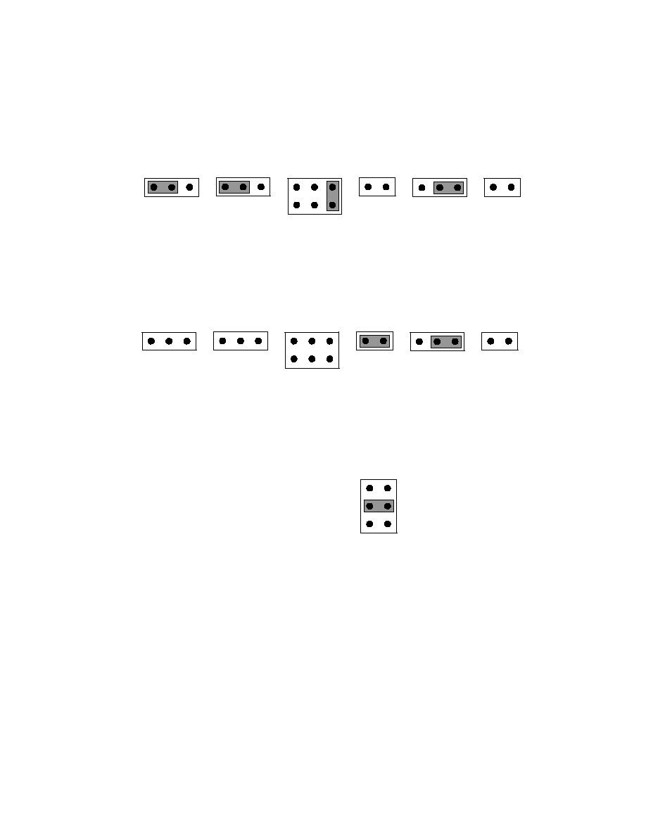
[SW3](MODE1): No.1 to 5 set the mode of AK4356 and No.6 to 8 set the mode of CS8412.
No.
Pin
OFF
ON
1
CAD1
2
CAD0
Chip address (2bit)
<default="00">
3
DIF0
4
DIF1
5
DIF2
Digital interface format of AK4356
(See table 2.)
6
M2
7
M1
8
M0
Digital interface format of CS8414
(See table 2.)
(Note)
Table 3. SW3 set-up
(Note: M2-0 should be selected at only evaluation mode 1.
In other mode, these should be "OFF".)
3
4
5
6
7
8
JP6
Mode
Format
DIF0
DIF1
DIF2
M2
M1
M0
BICK2
0
16bit, LSB justified
0
0
0
1
0
1
THR
1
20bit, LSB justified
1
0
0
-
-
-
-
2
24bit, MSB justified
0
1
0
0
0
0
INV
3
I2S
1
1
0
0
1
0
THR
default
4
24bit, LSB justified
0
0
1
-
-
-
-
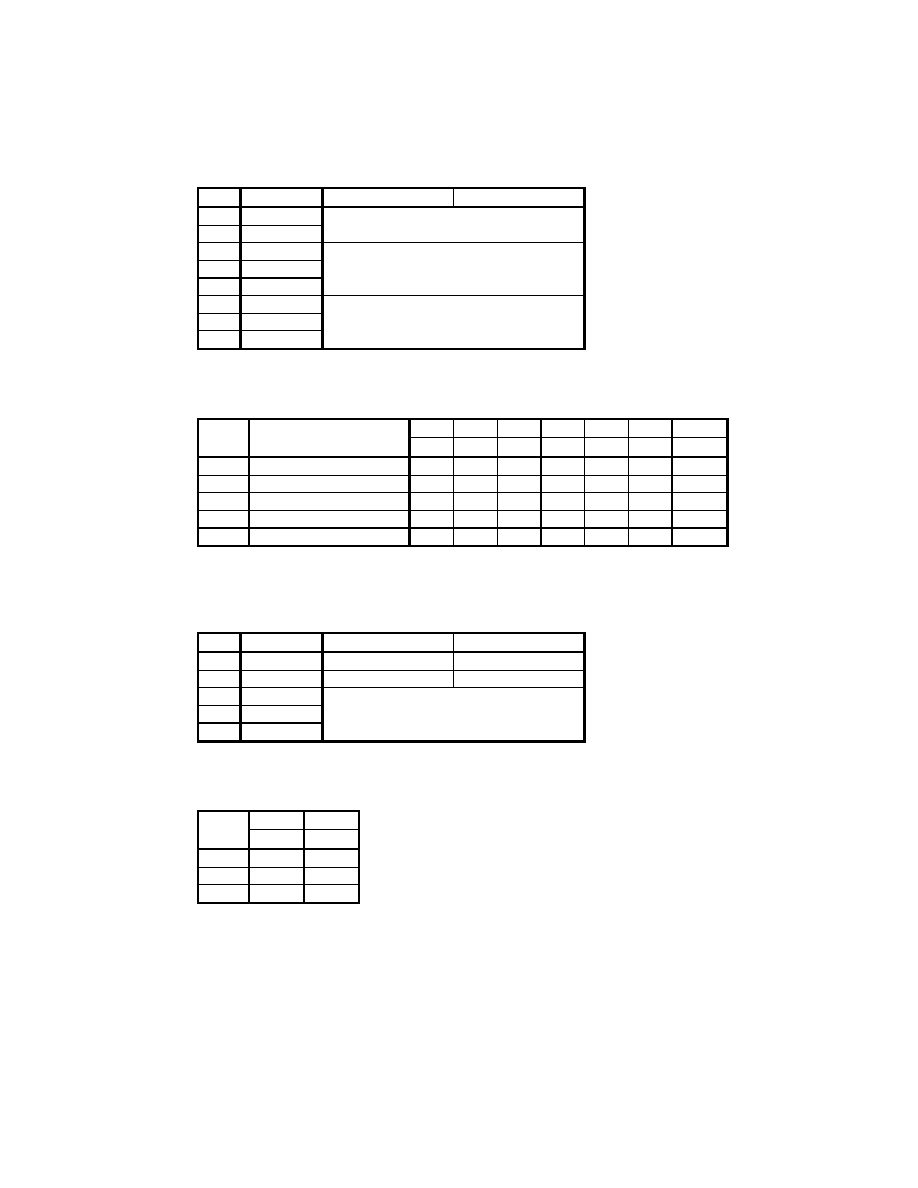
Table 4. Digital interface format set-up (1=ON, 0=OFF)
(CS8414 does not correspond to 20/24bit LSB justified format.)
[SW4](MODE2): Set the mode of AK4356.
No.
Pin
OFF <default>
ON
1
DFS0
Normal speed
Double speed
2
DZFE
Zero detect disable
Zero detect enable
3
CKS2
4
CKS1
5
CKS0
Clock select
(See the datasheet of AK4356.
JP5 and 8 should be selected as table 4.)
Table 5. SW4 set-up
[JP5, 8]: Set the dividing rate corresponding to CKS2-0. This set up is needed only for the evaluation mode 3.
JP5
JP8
Mode
FS2
FS1
128fs
x1/2
x1
256fs
x1
x1
512fs
x1
x2
Table 6. JP5 and 8 set up
(For 192fs/384fs/768fs mode, use the external divider.)